- Measured quantities
- Sheet resistance, resistivity, conductivity and plain resistance, shown together
- Probe geometry
- Four in-line probes, 1 mm, 2 mm or 4 mm spacing depending on the head fitted
- Resistance range
- 100 µΩ to 100 kΩ on the compact model; 1 µΩ to 100 MΩ on the widest
- Sheet resistance accuracy
- 3% on three models; 4% on the low-resistance model; 5% above 2 MΩ
- Resistance accuracy
- 0.05% in the middle of the range; 0.2% at the bottom; up to 0.5% at the top
- Test current
- ≤10 mA, ≤100 mA or ≤500 mA depending on model
- Thickness correction
- Sample thickness entered once, so resistivity is computed without a lookup table
- Dual measurement mode
- Fitted on three models, to correct probe drift and edge effects
- Interfaces
- HANDLER, RS232, RS485, USB host and USB device
A sheet of conductive film has no length and no width that matter. What it has is a resistance per square, and that is the number a coating line, a wafer fab or a photovoltaic process is actually controlling. Measuring it takes four points on the surface, not two clips on the ends.
Product overview
These are bench instruments for sheet resistance, resistivity and conductivity, with a plain resistance mode for bulk parts. Each one drives a current through the outer two probes of an in-line four-point head and reads the voltage across the inner two.
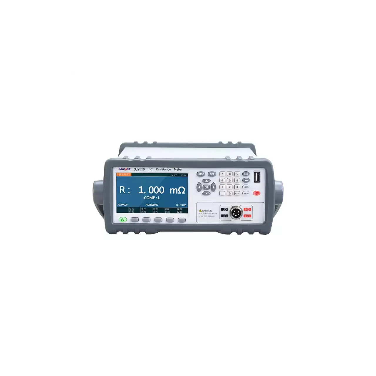
Four models cover the range. The compact one reads 100 µΩ to 100 kΩ on a 4.3-inch screen. The three larger ones run from 10 µΩ to 1 MΩ, from 1 µΩ to 20 kΩ, and from 1 µΩ to 100 MΩ, with 7-inch screens and a dual measurement mode that corrects probe drift and edge effects. Sheet resistance accuracy is quoted separately from resistance accuracy, at 3% or 4%, because it depends on geometry as well as on the electronics.
All four take the same probe heads and the same stand, measure temperature alongside the electrical result, and carry HANDLER, RS232, RS485 and USB host as standard.
How the four-point probe tester works
Four probes are pressed onto the surface in a line, equally spaced. The outer two carry a known current; the inner two measure the voltage that current produces between them. Because the voltage probes draw almost no current, the contact resistance under those two tips does not enter the reading, and the probe resistance does not either.
For a layer thin compared with the probe spacing, the sheet resistance is proportional to the measured voltage divided by the current, with a constant fixed by the geometry. The instrument applies that constant, so the display reads in ohms per square. When the layer is not thin compared with the spacing, or the sample is small, a correction factor applies, and that is where the dual measurement mode and the correct probe spacing earn their place.
Resistivity follows from the sheet resistance multiplied by the thickness. The thickness is entered before the run, which is why the instrument can show resistivity directly instead of asking the operator to multiply afterwards. Conductivity is its reciprocal, displayed in siemens per unit length.
How to select the right four-point probe tester
Start with the sheet resistance window. Coated glass and thin metal films sit in the low ohms per square and suit the low-resistance model; semiconductor layers and lightly doped films sit higher and need the wide-range model; a laboratory that sees both needs the wide one and should accept its coarser accuracy at the extremes.
Then the material, because it fixes the probe head. Tungsten carbide at 1 mm for hard wafers, beryllium copper at 2 mm for metals and photovoltaic panels, 4 mm for larger samples, and a conductive rubber tip for films that a needle would pierce. The head, not the instrument, decides whether the sample survives the measurement.
Then the sample size against the probe spacing. A small coupon relative to the spacing needs a correction, and the models with the dual measurement mode handle it better. A 200 mm panel does not.
Then the thickness range. A resistivity reading is only as good as the thickness entered, and a sample whose thickness varies across its area will give a resistivity that varies for a reason the instrument cannot see.
Finally the output. A lab needs the display and the USB record; a coating line needs the handler or the serial link and a comparator with limits per product.
Measurement limitations and selection considerations
The measurement assumes a homogeneous layer. A coating with a resistive skin over a conductive base, or a wafer with an implant profile, is not a single sheet, and the four-point reading is an average of what the current path samples, weighted towards the surface.
Probe pressure matters. Too little and the contact is unstable; too much and a soft film is pierced or a thin wafer is cracked. The material gives no pressure figure, and the correct pressure depends on the tip and the sample, so it has to be established on the material itself.
The reading is at the surface, under the probes. A sample that has just been handled, cleaned or coated may still be changing; the temperature and humidity readout is there to make that visible, and the temperature compensation only corrects a number, not the drift.
Edge effects are the largest source of error on small samples. Current spreading near an edge lowers the apparent sheet resistance, and the correction depends on the distance from the probe to the edge. A fixture that places the probes at a repeatable distance from the edge is worth more than a better instrument.
Finally, this is not a mapping instrument. It measures where the probes are placed; a wafer or a panel has a distribution, and characterising that distribution needs a stage that moves the sample between readings.
Every value below is taken from source documentation. Where a parameter is not stated in the available material it is marked as information required rather than estimated.